| Email not displaying correctly? View it in your browser. |
 Volume
3 Issue 3 - March 2010
Volume
3 Issue 3 - March 2010 |
|
The NNN Newsletter
Manufacturing Challenges and Innovations: NNN Testimony on Capitol Hill
In his testimony to Congress, Tuominen cited the U.S. investment in nanotechnology through the National Nanotechnology Initiative resulting in enormous advancements in the ability to make, control, and utilize nanomaterials whose characteristic features are 1-100 nanometers. The last ten years in nanotechnology has been a period of dramatic discovery and exploration. Brilliant scientists and engineers from interdisciplinary teams have created proof-of-concept demonstrations with high performance nanoscale materials and devices. These results are now beginning to impact just about every commercial product sector, including electronics, materials, health, transportation, consumer care products, and energy. However, transitioning from proof-of-concept demonstration, to prototype, to manufacturing pilot, to full-scale manufacturing is not trivial. This is especially true in the case of an emergent field like nanotechnology, where, in most cases, we cannot simply adapt old designs of production tools for these new methods. Manufacturing brings to bear a new range of issues: process development and modeling, scale-up, metrology, process control, tooling, workforce, safety, and supply chain. Ultimately, these issues have to be addressed because, without manufacturing, there are no products. Perhaps more than any other previous activity, nanomanufacturing requires close cooperative efforts between industry, academia, and government.
Regards, Learn More about the
An Interview with Scott Rickert Dr. Scott Rickert�President, Co-founder, and CEO of Nanofilm �is one of the the top leaders of the Nanotechnology Community today. He was responsible for the original concepts that launched Nanofilm into the nanotechnology arena; was instrumental in the development of the company's first coating called "Clarity"; and continues to set the vision for the company's R&D team. In this interview, author Steve Waite talks to Dr. Rickert about his view of nanotechnology in the coming decade and the role of established companies, start-ups, academia and government. As you will see, Dr. Rickert believes nanotechnology is the software of the 21st century. The interview also explores the evolution of Nanofilm and discusses the company's prospects in the global marketplace. More... Nanopatterned Polymer Photovoltaic Heterojunction Using a Double Imprint Process
|
Upcoming Events April 5 - 9, 2010 April 11 - 16, 2010 April 12 - 16, 2010 April 14 - 15, 2010
Advertisement Upcoming Calls April 1, 2010 April 16, 2010 April 17, 2010 May 1, 2010
Advertisement Recently Published DNA-decorated Carbon-nanotube-based Chemical Sensors on Complementary Metal Oxide Semiconductor Circuitry Economic Assessment of Single-walled Carbon Nanotube Processes Design, Synthesis, and Characterization of a Persistent Nonacene Derivative
Advertisement Affiliated Centers |
||
|
The National Nanomanufacturing Network Newsletter Subscribe / Unsubscribe from this list. Our mailing address is: The National Nanomanufacturing Network 322 Lederle Graduate Research Center 710 N. Pleasant Street University of Massachusetts Amherst, MA 01003 Our email address is: nnn@nanomanufacturing.org Our phone number is: (413) 577-0570 Copyright (C) 2008 The National Nanomanufacturing Network All rights reserved. Supported by the National Science Foundation under Grant No. DMI-0531171. |
|||
 The federal government is presently considering approaches to bolster its role in supporting innovations in future manufacturing industries within the U.S. This month, Mark Tuominen, Director of the National Nanomanufacturing Network (NNN), along with industry colleagues, provided expert testimony to the House Science and Technology Committee at a hearing on the role of the federal government in supporting manufacturing innovation in the U.S. Tuominen spoke about the impact of present programs and methods, as well as significant opportunities for the federal government to enhance the transition of nanotechnology research and development to commercialization of next generation consumer products. The purpose of the testimony was to provide a boost for research and development in nanomanufacturing and further foster university-industry interactions to share information and transition technological advances.
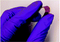 Polymer bulk heterojunction materials offer a potentially low-cost, facile approach for the fabrication of efficient photovoltaic (PV) devices. In order to optimize the efficiency of such materials systems, features must be synthesized balancing the tradeoffs associated with photon absorption, transport and charge separation of photogenerated excitons, and direct pathways for collection of electrons and holes. One approach to address these divergent design requirements is to devise an interpenetrating network of donor and acceptor materials having nanoscale features matching the typical exciton transport length on the order of 10 nm. Recently He et. al. investigated the use of nanoimprint lithography (NIL) as a method to form patterned polymer blends generating a three-dimensional interpenetrating hierarchy of electron donor and acceptor materials.