|
The NNN Newsletter
NENS 2010: Nanomanufacturing Stakeholders Provide Insights into Challenges, Benefits, and Societal Impact
 The New England Nanomanufacturing Summit 2010 (NENS 2010) held June 22-24 in Lowell, MA included technical discussions by scientists, experts, and industries in the field of nanomanufacturing by stakeholders from academic institutions, government, and industries in the Northeast, along with national and international participants. The event, sponsored by the National Nanomanufacturing Network and organized by the NSF Center for High-rate Nanomanufacturing (CHN) at Northeastern University, with partners University of Massachusetts Lowell and University of New Hampshire, along with the NSF Center for Hierarchical Manufacturing at the University of Massachusetts Amherst, provided topical presentations on emerging technologies, applications, and high impact, fundamental research. The New England Nanomanufacturing Summit 2010 (NENS 2010) held June 22-24 in Lowell, MA included technical discussions by scientists, experts, and industries in the field of nanomanufacturing by stakeholders from academic institutions, government, and industries in the Northeast, along with national and international participants. The event, sponsored by the National Nanomanufacturing Network and organized by the NSF Center for High-rate Nanomanufacturing (CHN) at Northeastern University, with partners University of Massachusetts Lowell and University of New Hampshire, along with the NSF Center for Hierarchical Manufacturing at the University of Massachusetts Amherst, provided topical presentations on emerging technologies, applications, and high impact, fundamental research.
The first day of the event focused on Nano Environmental Health and Safety (NanoEHS) topics including regulations of nanomaterials and consumer/worker protection challenges presented by the EPA and CDC/NIOSH respectively. The last 2 days focused on advanced process development, scaled production of nanomaterials, and applications such as energy and power, nanoelectronics, protective coatings, multiscale and ultra-high density nanopatterning, biosensors, and data storage.
The event provided key insights into challenges and potential benefits of nanotechnology and nanomanufacturing, and further engaged stakeholders and attendees in networking discussions and opportunities. Fostering such interactions enables broader understanding by all stakeholders and participants on the challenges associated with transitioning nanoscience research to commercially viable consumer products.
More...
Regards,
Jeff Morse, Managing Director,
National Nanomanufacturing Network
Learn More about the 
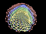
When Top-Down Meets Bottom-Up: EUV and X-ray Interference Lithography for Sub-20-nm Features
 After achieving the 45-nm process [1], today's semiconductor industry is nearing the 20-nm process and looking for techniques that would enable sub-22-nm-half-pitch line patterns [2]. Following the continuous increase in exposure tool numerical aperture (NA), researchers are pursuing reductions in exposure wavelengths. This effort had them look at extreme ultraviolet (EUV: 13.4 nm in wavelength) as an exposure light source. Unlike the numerical aperture engineering, change of a light source to EUV demands development of its related components, such as photoresist and optics. Until a reliable solution for EUV lithography is developed, EUV interference lithography (EUVIL) would not solely advance the lithographic technology but would also help to optimize photoresist materials for EUV. EUVIL is capable of patterning sub-20-nm features at large scales and, unlike hexagonal sub-20-nm features demonstrated by block copolymer lithography, can create diverse geometries from line/space to hexagonal to rectangular array of dots. EUVIL and XIL are noted as some of the next generation lithography techniques that are under active development. Demonstrated applications of these techniques encompass production of catalyst arrays, nanophotonic devices, nanoimprint stamps, holographic fabricaion of Fresnel zone plates, guided self-assembly of block copolymers and colloidal particles, nanoparticle arrays, chemical patterning of self-assembled monolayers and radiation grafting of polymer nanostructures. More.... After achieving the 45-nm process [1], today's semiconductor industry is nearing the 20-nm process and looking for techniques that would enable sub-22-nm-half-pitch line patterns [2]. Following the continuous increase in exposure tool numerical aperture (NA), researchers are pursuing reductions in exposure wavelengths. This effort had them look at extreme ultraviolet (EUV: 13.4 nm in wavelength) as an exposure light source. Unlike the numerical aperture engineering, change of a light source to EUV demands development of its related components, such as photoresist and optics. Until a reliable solution for EUV lithography is developed, EUV interference lithography (EUVIL) would not solely advance the lithographic technology but would also help to optimize photoresist materials for EUV. EUVIL is capable of patterning sub-20-nm features at large scales and, unlike hexagonal sub-20-nm features demonstrated by block copolymer lithography, can create diverse geometries from line/space to hexagonal to rectangular array of dots. EUVIL and XIL are noted as some of the next generation lithography techniques that are under active development. Demonstrated applications of these techniques encompass production of catalyst arrays, nanophotonic devices, nanoimprint stamps, holographic fabricaion of Fresnel zone plates, guided self-assembly of block copolymers and colloidal particles, nanoparticle arrays, chemical patterning of self-assembled monolayers and radiation grafting of polymer nanostructures. More....
NNI Strategic Planning Stakeholder Workshop To Take Place July 13 - 14, 2010
 The National Nanotechnology Initiative will hold a Strategic Planning Stakeholder Workhop on July 13 - 14, 2010, in Arlington, VA. This event is free, open to the public, and will be webcast for the benefit of those who are unable to attend. Complete Agenda and Confirmed Participants are available on the Workshop Web site. More.... The National Nanotechnology Initiative will hold a Strategic Planning Stakeholder Workhop on July 13 - 14, 2010, in Arlington, VA. This event is free, open to the public, and will be webcast for the benefit of those who are unable to attend. Complete Agenda and Confirmed Participants are available on the Workshop Web site. More....
New England Nano Event Addresses Environmental Health and Safety Topics
 The first day of NENS 2010 focused on Environmental Health and Safety issues associated with nanotechnology, providing presentations by leaders in the field from government, academic centers, industry consortia, and nonprofit organizations. Speakers included Kristan Markey from the Environmental Protection Agency (EPA), who discussed the challenges of risk assessment and regulation of nanomaterials, and further described the EPA�s approach to interacting with industry regarding emerging nanomaterials which includes a pre-manufacture notice where companies voluntarily supply the EPA with information on properties of their specific under the Toxic Substance Control Act (TSCA). Hilary Godwin from the University of California Center for Environmental Implications of Nanotechnology (UC CEIN) at UCLA discussed prevention-based approaches to managing the risks of nanomaterials. Paul Schulte of the Center for Disease Control/National Institute for Occupational Safety and Health presented a progress report on protecting the health and safety of nanomaterial workers. More.... The first day of NENS 2010 focused on Environmental Health and Safety issues associated with nanotechnology, providing presentations by leaders in the field from government, academic centers, industry consortia, and nonprofit organizations. Speakers included Kristan Markey from the Environmental Protection Agency (EPA), who discussed the challenges of risk assessment and regulation of nanomaterials, and further described the EPA�s approach to interacting with industry regarding emerging nanomaterials which includes a pre-manufacture notice where companies voluntarily supply the EPA with information on properties of their specific under the Toxic Substance Control Act (TSCA). Hilary Godwin from the University of California Center for Environmental Implications of Nanotechnology (UC CEIN) at UCLA discussed prevention-based approaches to managing the risks of nanomaterials. Paul Schulte of the Center for Disease Control/National Institute for Occupational Safety and Health presented a progress report on protecting the health and safety of nanomaterial workers. More....
Read more on 
|
Upcoming Events
July 1 - 2, 2010
Nanomedicine 2010
July 4 - 8, 2010
1st International Conference on Materials for Energy
July 11 - 16, 2010
Advances in Nonvolatile Memory Materials and Devices
July 13 - 15, 2010
SEMICON West 2010
July 18 - 23, 2010
Gordon Research Conference: Nanostructure Fabrication
July 21 - 23, 2010
Nanomaterials and Worker Health: Medical Surveillance, Exposure Registries, and Epidemiologic Research
View Full Calendar
Advertisement
Upcoming Calls
Through July 6, 2010
APCOT 2010 Postdeadline submissions for papers
July 30, 2010
3rd Annual Nanotechnology Symposium
Deadline for abstracts
July 30, 2010
Nanosafe 2010
Deadline for paper and poster abstracts
August 30, 2010
BIT's 1st Annual World Congress of Nanomedicine
Deadline for poster abstracts
Recently Published
From Our Affiliates
Toxicity of Carbon Nanotubes to the Activated Sludge Process
Journal of Hazardous Materials 178(1-3):356-362
Photooxidation of Nanopatterned Poly(chloromethylstyrene): Direct Formation of Cross linked Aldehyde-Functionalized Films for Chemical Functionalization and Bioconjugation
Macromolecular Rapid Communications 31(9):910-914
Gating of Single-Layer Graphene with Single-Stranded Deoxyribonucleic Acids
Small 6(10):1150-1155
Water Transport through Ultrathin Graphene
Journal of Physical Chemistry Letters 1(10):1590-1594
Catalytic and Molecular Beacons for Amplified Detection of Metal Ions and Organic Molecules with High Sensitivity
Analytical Chemistry 82(12):5005-5011
Affiliated Centers


|
 Volume
3 Issue 6 - June 2010
Volume
3 Issue 6 - June 2010